High-level architectural Requirements
- SMP Cache coherency (TileLink?)
- Minumum 800mhz
- Minimum 2-core SMP, more likely 4-core uniform design, each core with full 4-wide SIMD-style predicated ALUs
- 6GFLOPS single-precision FP
- 128 64-bit FP and 128 64-bit INT register files
- RV64GC compliance for running full GNU/Linux-based OS
- SimpleV compliance
- xBitManip (required for VPU and ideal for predication)
- On-chip tile buffer (memory-mapped SRAM), likely shared between all cores, for the collaborative creation of pixel "tiles".
- 4-lane 2Rx1W SRAMs for registers numbered 32 and above; Multi-R x Multi-W for registers 1-31. TODO: consider 2R for registers to be used as predication targets if >= 32.
- Idea: generic implementation of ports on register file so as to be able to experiment with different arrangements.
- Potentially: Lane-swapping / crossing / data-multiplexing bus on register data (particularly because of SHAPE-REMAP (1D/2D/3D)
- Potentially: Registers subdivided into 16-bit, to match elwidth down to 16-bit (for FP16). 8-bit elwidth only goes down as far as twin-SIMD (with predication). This requires registers to have extra hidden bits: register x30 is now "x30:0+x30.1+x30.2+x30.3". have to discuss.
See requirements specification
Conversation Notes
http://lists.libre-riscv.org/pipermail/libre-riscv-dev/2019-January/000310.html
We will need fast f32 <-> i16 at least since that is used for 16-bit z-buffers. Since we don't have indexed load/store and need to manually construct pointer vectors we will need fast i32 -> i64. We will also need fast i32 <-> f32.
'm thinking about using tilelink (or something similar) internally as having a cache-coherent protocol is required for implementing Vulkan (unless you want to turn off the cache for the GPU memory, which I don't think is a good idea), axi is not a cache-coherent protocol, and tilelink already has atomic rmw operations built into the protocol. We can use an axi to tilelink bridge to interface with the memory.
I'm thinking we will want to have a dual-core GPU since a single core with 4xSIMD is too slow to achieve 6GFLOPS with a reasonable clock speed. Additionally, that allows us to use an 800MHz core clock instead of the 1.6GHz we would otherwise need, allowing us to lower the core voltage and save power, since the power used is proportional to F*V2. (just guessing on clock speeds.)
I don't know about power, however I have done some research and a 4Kbyte (or 16, icr) SRAM (what I was thinking of for a tile buffer) takes in the ballpark of 1000 um2 in 28nm. Using a 4xFMA with a banked register file where the bank is selected by the lower order register number means we could probably get away with 1Rx1W SRAM as the backing memory for the register file, similarly to Hwacha. I would suggest 8 banks allowing us to do more in parallel since we could run other units in parallel with a 4xFMA. 8 banks would also allow us to clock gate the SRAM banks that are not in use for the current clock cycle allowing us to save more power. Note that the 4xFMA could be 4 separately allocated FMA units, it doesn't have to be SIMD style. If we have enough hw parallelism, we can under-volt and under-clock the GPU cores allowing for a more efficient GPU. If we are using the GPU cores as CPU cores as well, I think it would be important to be able to use a faster clock speed when not using the extended registers (similar to how Intel processors use a lower clock rate when AVX512 is in use) so that scalar code is not slowed down too much.
Using a 4xFMA with a banked register file where the bank is selected by the lower order register number means we could probably get away with 1Rx1W SRAM as the backing memory for the register file, similarly to Hwacha.
okaaay.... sooo... we make an assumption that the top higher "banks" are pretty much always going to be "vectorised", such that, actually, they genuinely don't need to be 6R-4W (or whatever).
Yeah pretty much, though I had meant the bank number comes from the least-significant bits of the 7-bit register number.
Assuming 64-bit operands: If you could organize 2 SRAM macros and use the pair of them to read/write 4 registers at a time (256-bits). The pipeline will allow you to dedicate 3 cycles for reading and 1 cycle for writing (4 registers each).
RS1 = Read of operand S1
WRd = Write of result Dst
FMx = Floating Point Multiplier, x = stage.

   |RS1|RS2|RS3|FWD|FM1|FM2|FM3|FM4|
                   |FWD|FM1|FM2|FM3|FM4|
                       |FWD|FM1|FM2|FM3|FM4|
                           |FWD|FM1|FM2|FM3|FM4|WRd|
                   |RS1|RS2|RS3|FWD|FM1|FM2|FM3|FM4|
                                   |FWD|FM1|FM2|FM3|FM4|
                                       |FWD|FM1|FM2|FM3|FM4|
                                           |FWD|FM1|FM2|FM3|FM4|WRd|
                                   |RS1|RS2|RS3|FWD|FM1|FM2|FM3|FM4|
                                                   |FWD|FM1|FM2|FM3|FM4|
                                                       |FWD|FM1|FM2|FM3|FM4|
                                                           |FWD|FM1|FM2|FM3|FM4|WRd|
The only trick is getting the read and write dedicated on different clocks. When the RS3 operand is not needed (60% of the time) you can use the time slot for reading or writing on behalf of memory refs; STs read, LDs write.
You will find doing VRFs a lot more compact this way. In GPU land we called the flip-flops orchestrating the timing "collectors".
Justification for Branch Prediction
http://lists.libre-riscv.org/pipermail/libre-riscv-dev/2018-December/000212.html
We can combine several branch predictors to make a decent predictor: call/return predictor -- important as it can predict calls and returns with around 99.8% accuracy loop predictor -- basically counts loop iterations some kind of global predictor -- handles everything else
We will also want a btb, a smaller one will work, it reduces average branch cycle count from 2-3 to 1 since it predicts which instructions are taken branches while the instructions are still being fetched, allowing the fetch to go to the target address on the next clock rather than having to wait for the fetched instructions to be decoded.
https://www.researchgate.net/publication/316727584_A_case_for_standard-cell_based_RAMs_in_highly-ported_superscalar_processor_structures
well, there is this concept: https://www.princeton.edu/~rblee/ELE572Papers/MultiBankRegFile_ISCA2000.pdf
it is a 2-level hierarchy for register cacheing. honestly, though, the reservation stations of the tomasulo algorithm are similar to a cache, although only of the intermediate results, not of the initial operands.
i have a feeling we should investigate putting a 2-level register cache in front of a multiplexed SRAM.
For GPU workloads FP64 is not common so I think having 1 FP64 alu would be sufficient. Since indexed loads and stores are not supported, it will be important to support 4x64 integer operations to generate addresses for loads/stores.
I was thinking we would use scoreboarding to keep track of operations and dependencies since it doesn't need a cam per alu. We should be able to design it to forward past the register file to allow for 0-latency forwarding. If we combined that with register renaming it should prevent most war and waw data hazards.
I think branch prediction will be essential if only to fetch and decode operations since it will reduce the branch penalty substantially.
Note that even if we have a zero-overhead loop extension, branch prediction will still be useful as we will want to be able to run code like compilers and standard RV code with decent performance. Additionally, quite a few shaders have branching in their internal loops so zero-overhead loops won't be able to fix all the branching problems.
you would need a 4-wide cdb anyway, since that's the performance we're trying for.
if the 32-bit ops can be grouped as 2x SIMD to a 64-bit-wide ALU, then only 2 such ALUs would be needed to give 4x 32-bit FP per cycle per core, which means only a 2-wide CDB, a heck of a lot better than 4.
oh: i thought of another way to cut the power-impact of the Reorder Buffer CAMs: a simple bit-field (a single-bit 2RWW memory, of address length equal to the number of registers, 2 is because of 2-issue).
the CAM of a ROB is on the instruction destination register. key: ROBnum, value: instr-dest-reg. if you have a bitfleid that says "this destreg has no ROB tag", it's dead-easy to check that bitfield, first.
Avoiding Memory Hazards
- WAR and WAR hazards through memory are eliminated with speculation because actual updating of memory occurs in order, when a store is at the head of the ROB, and hence, no earlier loads or stores can still be pending
- RAW hazards are maintained by two restrictions:
- not allowing a load to initiate the second step of its execution if any active ROB entry occupied by a store has a destination field that matches the value of the A field of the load and
- maintaining the program order for the computation of an effective address of a load with respect to all earlier stores
- These restrictions ensure that any load that access a memory location written to by an earlier store cannot perform the memory access until the store has written the data.
Advantages of Speculation, Load and Store hazards:
- A store updates memory only when it reached the head of the ROB
- WAW and WAR type of hazards are eliminated with speculation (actual updating of memory occurs in order)
- RAW hazards through memory are maintained by not allowing a load to initiate the second step of its execution
- Check if any store has a destination field that matched the
value of the load:
- SD F1 100(R2)
- LD F2 100(R2)
Exceptions
- Exceptions are handled by not recognising the exception until instruction that caused it is ready to commit in ROB (reaches head of ROB)
Reorder Buffer
- Results of an instruction become visible externally when it leaves
the ROB
- Registers updated
- Memory updated
Reorder Buffer Entry
- Instruction type
- branch (no destination resutl)
- store (has a memory address destination)
- register operation (ALU operation or load, which has reg dests)
- Destination
- register number (for loads and ALU ops) or
- memory address (for stores) where the result should be written
- Value
- value of instruction result, pending a commit
- Ready
- indicates that the instruction has completed execution: value is ready
Register Renaming resources
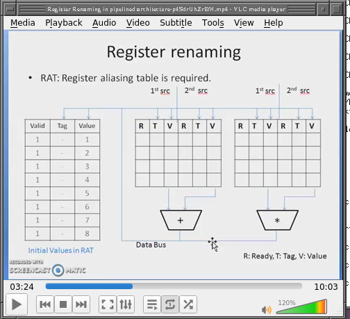
- https://www.youtube.com/watch?v=p4SdrUhZrBM
- https://www.d.umn.edu/~gshute/arch/register-renaming.xhtml
- ROBs + Rename http://euler.mat.uson.mx/~havillam/ca/CS323/0708.cs-323010.html
Video @ 3:24, "RAT" table - Register Aliasing Table:
This scheme looks very much like a Reservation Station.
There is another way to get precise ordering of the writes in a scoreboard. First, one has to implement forwarding in the scoreboard. Second, the function units need an output queue Now, one can launch an instruction and pick up its operand either from the RF or from the function unit output while the result sits in the function unit waiting for its GO_Write signal.
Thus the launching of instructions is not delayed due to hazards but the results are delivered to the RF in program order.
This looks surprisingly like a 'belt' at the end of the function unit.
https://salsa.debian.org/Kazan-team/kazan/blob/e4b516e29469e26146e717e0ef4b552efdac694b/docs/ALU%20lanes.svg
so, coming back to this diagram, i think if we stratify the Functional Units into lanes as well, we may get a multi-issue architecture.
the 6600 scoreboard rules - which are awesomely simple and actually involve D-Latches (3 gates) not flip-flops (10 gates) can be executed in parallel because there will be no overlap between stratified registers.
if using that odd-even / msw-lsw division (instead of modulo 4 on the register number) it will be more like a 2-issue for standard RV instructions and a 4-issue for when SV 32-bit ops are loop-generated.
by subdividing the registers into odd-even banks we will need a pair of (completely independent) register-renaming tables: https://libre-riscv.org/3d_gpu/rat_table.png
for SIMD'd operations, if we have the same type of reservation station queue as with Tomasulo, it can be augmented with the byte-mask: if the byte-masks in the queue of both the src and dest registers do not overlap, the operations may be done in parallel.
i still have not yet thought through how the Reorder Buffer would work: here, again, i am tempted to recommend that, again, we "stratify" the ROB into odd-even (modulo 2) or perhaps modulo 4, with 32 entries, however the CAM is only 4-bit or 3-bit wide.
if an instruction's destination register does not meet the modulo requirements, that ROB entry is left empty. this does mean that, for a 32-entry Reorder Buffer, if the stratification is 4-wide (modulo 4), and there are 4 sequential instructions that happen e.g. to have a destination of r4 for insn1, r24 for insn2, r16 for insn3.... etc. etc.... the ROB will only hold 8 such instructions
and that i think is perfectly fine, because, statistically, it'll balance out, and SV generates sequentially-incrementing instruction registers, so that is fine, too.
i'll keep working on diagrams, and also reading mitch alsup's chapters on the 6600. they're frickin awesome. the 6600 could do multi-issue LD and ST by way of having dedicated registers to LD and ST. X1-X5 were for ST, X6 and X7 for LD.
i took a shot at explaining this also on comp.arch today, and that allowed me to identify a problem with the proposed modulo-4 "lanes" stratification.
when a result is created in one lane, it may need to be passed to the next lane. that means that each of the other lanes needs to keep a watchful eye on when another lane updates the other regfiles (all 3 of them).
when an incoming update occurs, there may be up to 3 register writes (that need to be queued?) that need to be broadcast (written) into reservation stations.
what i'm not sure of is: can data consistency be preserved, even if there's a delay? my big concern is that during the time where the data is broadcast from one lane, the head of the ROB arrives at that instruction (which is the "commit" condition), it gets committed, then, unfortunately, the same ROB# gets reused.
now that i think about it, as long as the length of the queue is below the size of the Reorder Buffer (preferably well below), and as long as it's guaranteed to be emptied by the time the ROB cycles through the whole buffer, it should be okay.
Don't forget that in these days of Spectre and Meltdown, merely preventing dead instruction results from being written to registers or memory is NOT ENOUGH. You also need to prevent load instructions from altering cache and branch instructions from altering branch prediction state.
Which, oddly enough, provides a necessity for being able to consume multiple containers from the cache Miss buffers, which oddly enough, are what makes a crucial mechanism in the Virtual Vector Method work.
In the past, one would forward the demand container to the waiting memref and then write the whole the line into the cache. S&M means you have to forward multiple times from the miss buffers and avoid damaging the cache until the instruction retires. VVM uses this to avoid having a vector strip mine the data cache.
I meant the renaming done as part of the SV extension, not the microarchitectural renaming.
ah ok, yes. right. ok, so i don't know what to name that, and i'd been thinking of it in terms of "post-renaming", as in my mind, it's not really renaming, at all, it's... remapping. or, vector "elements".
as in: architecturally we already have a name (vector "elements"). physically we already have a name: register file.
i was initially thinking that the issue stage would take care of it, by producing:
- post-remapped elements which are basically post-remapped register indices
- a byte-mask indicating which bytes of the register are to be modified and which left alone
- an element-width that is effectively an augmentation of (part of) the opcode
the element width goes into the ALU as an augmentation of the opcode because the 64-bit "register" now contains e.g. 16-bit "elements" indexed 0-3, or 8-bit "elements" indexed 0-7, and we now want a SIMD-style (predicated) operation to take place.
now that i think about it, i think we may need to have the three phases be part of a pipeline, in a single dependency matrix.
I had a state machine in one chip that could come up out of power on in a state it could not get out of. Since this experience, I have a rule with state machines, A state machine must be able to go from any state to idle when the reset line is asserted.
You have to prove that the logic can never create a circular dependency, not a proof with test vectors, a logical proof like what we do with FP arithmetic these days.
however... we don't mind that, as the vectorisation engine will be, for the most part, generating sequentially-increasing index dest and src registers, so we kinda get away with it.
In this case:: you could simply design a 1R or 1W file (A.K.A. SRAM) and read 4 registers at a time or write 4 registers at a time. Timing looks like:
     |RdS1|RdS2|RdS3|WtRd|RdS1|RdS2|RdS3|WtRd|RdS1|RdS2|RdS3|WtRd|
                    |F123|F123|F123|F123|
                         |Esk1|EsK2|EsK3|EsK4|
                                        |EfK1|EfK2|EfK3|EfK4|
4 cycle FU shown. Read as much as you need in 4 cycles for one operand, Read as much as you need in 4 cycles for another operand, read as much as you need in 4 cycles for the last operand, then write as much as you can for the result. This simply requires flip-flops to capture the width and then deliver operands in parallel (serial to parallel converter) and similarly for writing.
discussion of how to do dest-latches rather than src-latches.
also includes need for forwarding to achieve it (synonymous with Tomasulo CDB).
also, assigning a result number at issue time allows multiple results to be stored-and-forwarded, meaning that multiplying up the FUs is not needed.
also, discussion of how to have multiple instructions issued even with the same dest reg: drop the reg-store and effectively rename them to "R.FU#". exceptions under discussion.
Speculation
https://groups.google.com/forum/#!topic/comp.arch/mzXXTU2GUSo
There is a minimal partial order that is immune to Spetré amd friends, You have the dependence matrix that imposes a minimal partial order on executing instructions (at least in the architecture you have been discussing herein) You just have to prove that your matrix provides that minimal partial order for instructions.
Then you have to prove that no cache/tlb state can be updated prior to the causing instruction being made retirable (not retired retirable).
As to cache updates, all "reasonable" interfaces that service cache misses will have line buffers to deal with the inbound and outbound memory traffic. These buffers will provide the appropriate data to the execution stream, but not update the cache until the causing instruction becomes transitively retirable. This will put "a little" extra pressure on these buffers.
As to the TLB it is easy enough on a TLB miss to fetch the mapping tables transitively and arrive at a PTE. This PTE cannot be installed until the causing instruction becomes retirable. The miss buffers are probably the right place, and if a second TLB miss occurs, you might just as well walk the tables again and if it hits the line in the buffer use the data from there. When we looked at this a long time ago, there was little benefit for being able to walk more than one TLB miss at a time.
|           3      |           2      |           1      |           0      |
| ---------------- | ---------------- | ---------------- | ---------------- |
|                  | xxxxxxxxxxxxxxaa | xxxxxxxxxxxxxxaa | XXXXXXXXXX011111 |
|                  | xxxxxxxxxxxxxxxx | xxxxxxxxxxxbbb11 | XXXXXXXXXX011111 |
|                  | xxxxxxxxxxxxxxaa | XXXXXXXXXX011111 | XXXXXXXXXX011111 |
| xxxxxxxxxxxxxxaa | xxxxxxxxxxxxxxaa | XXXXXXXXXXXXXXXX | XXXXXXXXX0111111 |
| xxxxxxxxxxxxxxxx | xxxxxxxxxxxbbb11 | XXXXXXXXXXXXXXXX | XXXXXXXXX0111111 |
2x16-bit / 32-bit:

| 9 8   | 7 6 5 |     4 3 |     2 1 | 0 |
| ----- | ----- | ------- | ------- | - |
| elwid | VL    | rs[6:5] | rd[6:5] | 0 |

| 9 8 7 6 5 |      4 3 |   2 |   1 | 0 |
| --------- | -------- | --- | --- | - |
| predicate | predtarg | end | inv | 1 |


|                  | xxxxxxxxxxxxxxxx | xxxxxxxxxxxbbb11 | XXXXXXXXXX011111 |
|                  | xxxxxxxxxxxxxxaa | XXXXXXXXXX011111 | XXXXXXXXXX011111 |
| xxxxxxxxxxxxxxaa | xxxxxxxxxxxxxxaa | XXXXXXXXXXXXXXXX | XXXXXXXXX0111111 |
| xxxxxxxxxxxxxxxx | xxxxxxxxxxxbbb11 | XXXXXXXXXXXXXXXX | XXXXXXXXX0111111 |
MVX and other reg-shuffling
> Crucial strategic op missing is MVX:
> regs[rd]= regs[regs[rs1]]
>
we could modify the definition slightly:
for i in 0..VL {
    let offset = regs[rs1 + i];
    // we could also limit on out-of-range
    assert!(offset < VL); // trap on fail
    regs[rd + i] = regs[rs2 + offset];
}

The dependency matrix would have the instruction depend on everything from
rs2 to rs2 + VL and we let the execution unit figure it out. for
simplicity, we could extend the dependencies to a power of 2 or something.

We should add some constrained swizzle instructions for the more
pipeline-friendly cases. One that will be important is:
for i in (0..VL) {
    let i = i * 4;
    let s1: [0; 4];
    for j in 0..4 {
        s1[j] = regs[rs1 + i + j];
    }
    for j in 0..4 {
        regs[rd + i + j] = s1[(imm >> j * 2) & 0x3];
    }
}
Another is matrix transpose for (2-4)x(2-4) matrices which we can implement
as similar to a strided ld/st except for registers.
TLBs / Virtual Memory
We were specifically looking for ways to not need large CAMs since they are power-hungry when designing the instruction scheduling logic, so it may be a good idea to have a smaller L1 TLB and a larger, slower, more power-efficient, L2 TLB. I would have the L1 be 4-32 entries and the L2 can be 32-128 as long as the L2 cam isn't being activated every clock cycle. We can also share the L2 between the instruction and data caches.
Register File having same-cycle "forwarding"
discussion about CDC 6600 Register File: it was capable of forwarding operands being written out to "reads", in the same cycle. this effectively turns the Reg File into a "Forwarding Bus".
we aim to only have (4 banks of) 2R1W ported register files, with additional Forwarding Multiplexers (which look exactly like multi-port regfile gate logic).
suggestion by Mitch is to have a "demon" on the front of the regfile, https://groups.google.com/d/msg/comp.arch/gedwgWzCK4A/qY2SYjd2DgAJ, which:
basically, you are going to end up with a "demon" at the RF and when
all read reservations have been satisfied the demon determines if the
result needs to be written to the RF or discarded. The demon sees
the instruction issue process, the branch resolutions, and the FU
exceptions, and keeps track of whether the result needs to be written.
It then forwards the result from the FU and clears the slot, then writes
the result to the RF if needed.
Design Layout
ok,so continuing some thoughts-in-order notes:
Scoreboards
scoreboards are not just scoreboards, they are dependency matrices, and there are several of them:
- one for LOAD/STORE-to-LOAD/STORE
- most recent LOADs prevent later STOREs
- most recent STOREs prevent later LOADs.
- a separate process analyses LOAD-STORE addresses for conflicts, based on sufficient bits to assess uniqueness as opposed to precise and exact matches
- one for Function-Unit to Function-Unit.
- it expresses both RAW and WAW hazards through "Go_Write" and "Go_Read" signals, which are stopped from proceeding by dependent 1-bit CAM latches
- exceptions may ALSO be made "precise" by holding a "Write prevention" signal. only when the Function Unit knows that an exception is not going to occur (memory has been fetched, for example), does it release the signal
- speculative branch execution likewise may hold a "Write prevention", however it also needs a "Go die" signal, to clear out the incorrectly-taken branch.
- LOADs/STOREs also must be considered as "Functional Units" and thus must also have corresponding entries (plural) in the FU-to-FU Matrix
- it is permitted for ALUs to BEGIN execution (read operands are valid) without being permitted to COMMIT. thus, each FU must store (buffer) results, until such time as a "commit" signal is received
- we may need to express an inter-dependence on the instruction order (raising the WAW hazard line to do so) as a way to preserve execution order. only the oldest instructions will have this flag dropped, permitting execution that has begun to also reach "commit" phase.
- one for Function-Unit to Registers.
- it expresses the read and write requirements: the source and destination registers on which the operation depends. source registers are marked "need read", dest registers marked "need write".
- by having more than one Functional Unit matrix row per ALU it becomes possible to effectively achieve "Reservation Stations" orthogonality with the Tomasulo Algorithm. the FU row must, like RS's, take and store a copy of the src register values.
Register Renaming
There are several potential well-known schemes for register-renaming: none of them will be used here. The scheme below is a new form of renaming that is a topologically and functionally direct equivalent of the Tomasulo Algorithm with a Reorder Buffer, that came from the "Register Alias Table" concept that is better suited to Scoreboards. It works by flattening out Reservation Stations to one per FU (requiring more FUs as a result). On top of this the function normally carried out by "tags" of the RAT table may be merged-morphed into the role carried out by the ROB Destination Register CAM which may be merged-morphed into a single vector (per register) of 1-bit mutually-exclusive "CAMs" that are added, very simply, to the FU-Register Dependency Matrix.
In this way, exactly as in the Tomasulo Algorithm, there is absolutely no need whatsoever for a separate PRF-ARF scheme. The PRF is the ARF.
Register-renaming will be done with a single extra mutually-exclusive bit in the FUxReg Dependency Matrix, which may be set on only one FU (per register). This bit indicates which of the FUs has the most recent destination register value pending. It is directly functionally equivalent to the Reorder Buffer Dest Reg# CAM value, except that now it is a string of 1-bit "CAMs".
When an FU needs a src reg and finds that it needs to create a dependency waiting for a result to be created, it must use this bit to determine which FU it creates a dependency on.
If there is a destination register that already has a bit set (anywhere in the column), it is cleared and replaced with a bit in the FU's row and the destination register's column.
See https://groups.google.com/d/msg/comp.arch/w5fUBkrcw-s/c80jRn4PCQAJ
MUL r1, r2, r3
FU name  Reg name
         12345678
add-0    ........
add-1    ........
mul-0    X.......
mul-1    ........
ADD r4, r1, r3
FU name  Reg name
         12345678
add-0    ...X....
add-1    ........
mul-0    X.......
mul-1    ........
ADD r1, r5, r6
FU name  Reg name
         12345678
add-0    ...X....
add-1    X.......
mul-0    ........
mul-1    ........
note how on the 3rd instruction, the (mul-0,R1) entry is cleared and replaced with an (add-1,R1) entry. future instructions now know that if their src operands require R1, they are to place a RaW dependency on add-1, not mul-0
Multi-issue
we may potentially have 2-issue (or 4-issue) and a simpler issue and detection by "striping" the register file according to modulo 2 (or 4) on the destination register number
- the Function Unit rows are multiplied up by 2 (or 4) however they are actually connected to the same ALUs (pipelined and with both src and dest register buffers/latches).
- the Register Read and Write signals are then "striped" such that read/write requests for every 2nd (or 4th) register are "grouped" and will have to fight for access to a multiplexer in order to access registers that do not have the same modulo 2 (or 4) match.
- we MAY potentially be able to drop the destination (write) multiplexer(s) by only permitting FU rows with the same modulo to write to that destination bank. FUs with indices 0,4,8,12 may only write to registers similarly numbered.
- there will therefore be FOUR separate register-data buses, with (at least) the Read buses multiplexed so that all FU banks may read all src registers (even if there is contention for the multiplexers)
FU-to-Register address de-muxed already
an oddity / artefact of the FU-to-Registers Dependency Matrix is that the write/read enable signals already exist as single-bits. "normal" processors store the src/dest registers as an index (5 bits == 0-31), where in this design, that has been expanded out to 32 individual Read/Write wires, already.
- the register file verilog implementation therefore must take in an array of 128-bit write-enable and 128-bit read-enable signals.
- however the data buses will be multiplexed modulo 2 (or 4) according to the lower bits of the register number, in order to cross "lanes".
FU "Grouping"
with so many Function Units in RISC-V (dozens of instructions, times 2 to provide Reservation Stations, times 2 OR 4 for dual (or quad) issue), we almost certainly are going to have to deploy a "grouping" scheme:
- rather than dedicate 2x4 FUs to ADD, 2x4 FUs to SUB, 2x4 FUs to MUL etc., instead we group the FUs by how many src and dest registers are required, and pass the opcode down to them
- only FUs with the exact same number (and type) of register profile will receive like-minded opcodes.
- when src and dest are free for a particular op (and an ALU pipeline is not stalled) the FU is at liberty to push the operands into the appropriate free ALU.
- FUs therefore only really express the register, memory, and execution dependencies: they don't actually do the execution.
Recommendations
- Include a merged address-generator in the INT ALU
- Have simple ALU units duplicated and allow more than one FU to receive (and process) the src operands.
Register file workloads
Note: Vectorisation also includes predication, which is one extra integer read
Integer workloads:
- 43% Integer
- 21% Load
- 12% store
24% branch
100% of the instruction stream can be integer instructions
- 75% utilize two source operand registers.
- 50% of the instruction stream can be Load instructions
- 25% can be store instructions,
- 25% can be branch instructions
FP workloads:
- 30% Integer
- 25% Load
- 10% Store
- 13% Multiplication
- 17% Addition
- 5% branch
in particular i found it fascinating that analysis of INT instructions found a 50% LD, 25% ST and 25% branch, and that 70% were 2-src ops. therefore you made sure that the number of read and write ports matched these, to ensure no bottlenecks, bearing in mind that ST requires reading an address and a data register.
I never had a problem in "reading the write slot" in any of my pipelines. That is, take a pipeline where LD (cache hit) has a latency of 3 cycles (AGEN, Cache, Align). Align would be in the cycle where the data was being forwarded, and the subsequent cycle, data could be written into the RF.
|dec|AGN|$$$|ALN|LDW|
For stores I would read the LDs write slot Align the store data and merge into the cache as::
|dec|AGEN|tag|---|STR|ALN|$$$|
You know 4 cycles in advance that a store is coming, 2 cycles after hit so there is easy logic to decide to read the write slot (or not), and it costs 2 address comparators to disambiguate this short shadow in the pipeline.
This is a lower expense than building another read port into the RF, in both area and power, and uses the pipeline efficiently.
Explicit Vector Length (EVL) extension to LLVM
- https://reviews.llvm.org/D57504
- http://lists.libre-riscv.org/pipermail/libre-riscv-dev/2019-January/000433.html
- http://lists.llvm.org/pipermail/llvm-dev/2019-January/129822.html
References
- https://en.wikipedia.org/wiki/Tomasulo_algorithm
- https://en.wikipedia.org/wiki/Reservation_station
- https://en.wikipedia.org/wiki/Register_renaming points out that reservation stations take a lot of power.
- http://home.deib.polimi.it/silvano/FilePDF/AAC/Lesson_4_ILP_PartII_Scoreboard.pdf scoreboarding
- MESI cache protocol, python https://github.com/sunkarapk/mesi-cache.git https://github.com/afwolfe/mesi-simulator
- https://kshitizdange.github.io/418CacheSim/final-report report on types of caches
- https://github.com/ssc3?tab=repositories interesting stuff
- https://en.wikipedia.org/wiki/Classic_RISC_pipeline#Solution_A._Bypassing pipeline bypassing
- http://ece-research.unm.edu/jimp/611/slides/chap4_7.html Tomasulo / Reorder
- Register File Bank Cacheing https://www.princeton.edu/~rblee/ELE572Papers/MultiBankRegFile_ISCA2000.pdf
- Discussion http://lists.libre-riscv.org/pipermail/libre-riscv-dev/2018-November/000157.html
- https://github.com/UCSBarchlab/PyRTL/blob/master/examples/example5-instrospection.py
- https://github.com/ataradov/riscv/blob/master/rtl/riscv_core.v#L210
- https://www.eda.ncsu.edu/wiki/FreePDK