Shakti M-Class Libre SoC
This SoC is a propsed libre design that draws in expertise from mass-volume SoCs of the past six years and beyond, and is being designed to cover just as wide a range of target embedded / low-power / industrial markets as those SoCs. Pincount is to be kept low in order to reduce cost as well as increase yields.
- See http://rise.cse.iitm.ac.in/shakti.html M-Class for top-level
- See pinouts for auto-generated table of pinouts (including mux)
- See peripheralschematics for example Reference Layouts
- See ramanalysis for a comprehensive analysis of why DDR3 is to be used.
- See todo for a rough list of tasks (and link to bugtracker)
- https://bugs.libre-soc.org/show_bug.cgi?id=2
Rough specification.
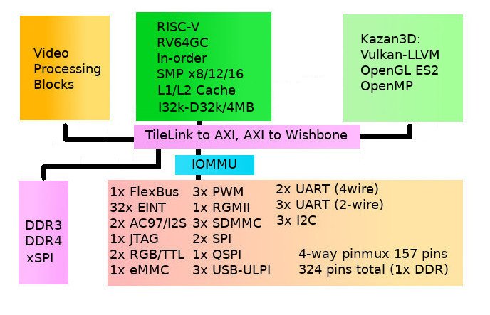
Quad-core 28nm OpenPOWER 64-bit (OpenPOWER v3.0B core with Simple-V Vector Media / 3D extensions), 300-pin 15x15mm BGA 0.8mm pitch, 32-bit DDR3-4/LPDDR3/4 memory interface and libre / open interfaces and accelerated hardware functions suitable for the higher-end, low-power, embedded, industrial and mobile space.
A 0.8mm pitch BGA allows relatively large (low-cost) VIA drill sizes to be used (8-10mil) and 4-5mil tracks with 4mil clearance. For details see http://processors.wiki.ti.com/index.php/General_hardware_design/BGA_PCB_design
Die area estimates
- http://hwacha.org/papers/riscv-esscirc2014-talk.pdf
- 40nm 64-bit rocket single-core single-issue in-order: 0.14mm2
- 40nm 16-16k L1 caches, 0.25mm2
- http://people.csail.mit.edu/beckmann/publications/tech.../grain_size_tr_feb_2010.pdf
Targetting full Libre Licensing to the bedrock.
The only barrier to being able to replicate the masks from scratch is the proprietary cells (e.g. memory cells) designed by the Foundries: there is a potential long-term strategy in place to deal with that issue.
The only proprietary interface utilised in the entire SoC is the DDR3/4 PHY plus Controller, which will be replaced in a future revision, making the entire SoC exclusively designed and made from fully libre-licensed BSD and LGPL openly and freely accessible VLSI and VHDL source.
In addition, no proprietary firmware whatsoever will be required to operate or boot the device right from the bedrock: the entire software stack will also be libre-licensed (even for programming the initial proprietary DDR3/4 PHY+Controller)
Inspiration from several sources
The design of this SoC is drawn from at least the following SoCs, which have significant multiplexing for pinouts, reducing pincount whilst at the same time permitting the SoC to be utilised across a very wide range of markets:
- A10/A20 EVB http://hands.com/~lkcl/eoma/A10-EVB-V1-2-20110726.pdf
- RK3288 T-Firefly http://www.t-firefly.com/download/firefly-rk3288/hardware/FR_RK3288_0930.pdf
- Ingenic JZ4760B ftp://ftp.ingenic.cn/SOC/JZ4760B/JZ4760B_DS_REVISION.PDF LEPUS Board ftp://ftp.ingenic.cn/DevSupport/Hardware/RD4760B_LEPUS/RD4760B_LEPUS_V1.3.2.PDF
- GPL-violating CT-PC89e http://hands.com/~lkcl/seatron/, and http://lkcl.net/arm_systems/CT-PC89E/ this was an 8.9in netbook weighing only 0.72kg and having a 3 HOUR battery life on a single 2100mAh cell, its casework alone inspired a decade of copycat china clone netbooks as it was slowly morphed from its original 8.9in up to (currently) an 11in form-factor almost a decade later in 2017.
- A64 Reference Designs for example this: http://linux-sunxi.org/images/3/32/Banana_pi_BPI-M64-V1_1-Release_201609.pdf
TI Boards such as the BeagleXXXX Series, or the Freescale iMX6 WandBoard etc., are, whilst interesting, have a different kind of focus and "feel" about them, as they are typically designed by Western firms with less access or knowledge of the kinds of low-cost tricks deployed to ingenious and successful effect by Chinese Design Houses. Not only that but they typically know the best components to buy. Western-designed PCBs typically source exclusively from Digikey, AVNet, Mouser etc. and the prices are often two to TEN times more costly as a result.
The TI and Freescale (now NXP) series SoCs themselves are also just as interesting to study, but again have a subtly different focus: cost of manufacture of PCBs utilising them not being one of those primary focii. Freescale's iMX6 is well-known for its awesome intended lifespan and support: ninteen years. That does however have some unintended knock-on effects on its pricing.
Instead, the primary input is taken from Chinese-designed SoCs, where cost and ease of production, manufacturing and design of a PCB using the planned SoC, as well as support for high-volume mass-produced peripherals is firmly a priority focus.
Target Markets
- EOMA68 Computer Card form-factor (general-purpose, eco-conscious)
- Smartphone / Tablet (basically the same thing, different LCD/CTP size)
- Low-end (ChromeOS style) laptop
- Industrial uses when augmented by a suitable MCU (for ADC/DAC/CAN etc.)
Common Peripherals to majority of target markets
- SPI or 8080 or RGB/TTL or LVDS LCD display. SPI: 320x240. LVDS: 1440x900.
- LCD Backlight, requires GPIO power-control plus PWM for brightness control
- USB-OTG Port (OTG-Host, OTG Client, Charging capability)
- Baseband Modem (GSM / GPRS / 3G / LTE) requiring USB, UART, and PCM audio
- Bluetooth, requires either full UART or SD/MMC or USB, plus control GPIO
- WIFI, requires either USB (but with power penalties) or better SD/MMC
- SD/MMC for external MicroSD
- SD/MMC for on-PCB eMMC (care needed on power/boot sequence)
- NAND Flash (not recommended), requires 8080/ATI-style Bus with dedicated CS#
- Optional 4-wire QSPI NAND/NOR for boot (XIP - Execute In-place - recommended).
- Audio over I2S (5-pin: 4 for output, 1 for input), fall-back to USB Audio
- Audio also over AC97
- Some additional SPI peripherals, e.g. connection to low-power MCU.
- GPIO (EINT-capable, with wakeup) for buttons, power, volume etc.
- Camera(s) either by CSI-1 (parallel CSI) or better by USB
- I2C sensors: accelerometer, compass, etc. Each requires EINT and RST GPIO.
- Capacitive Touchpanel (I2C and also requiring EINT and RST GPIO)
- Real-time Clock (usually an I2C device but may be on-board a support MCU)
- PCIe via PXPIPE
- LPC from Raptor Engineering
- USB3
- RGMII Gigabit Ethernet
Peripherals unique to laptop market
- Keyboard (USB or keyboard-matrix managed by MCU)
- USB, I2C or SPI Mouse-trackpad (plus button GPIO, EINT capable)
Peripherals common to laptop and Industrial Market
- Ethernet (RGMII or better 8080-style XT/AT/ATI MCU bus for e.g. DM9000)
Augmentation by an embedded MCU
Some functions, particularly analog, are particularly tricky to implement in an early SoC. In addition, CAN is still patented (not any more). For unusual, patented or analog functionality such as RTC, ADC, DAC, SPDIF, One-wire Bus and so on it is easier and simpler to deploy an ultra-low-cost low-speed companion Micro-Controller such as the crystal-less STMS8003 ($0.24) or the crystal-less STM32F072 or other suitable MCU, depending on requirements. For high-speed interconnect it may be wired up as an SPI device, and for lower-speed communication UART would be the simplest and easiest means of two-way communication.
This technique can be deployed in all scenarios (phone, tablet, laptop, industrial), and is an extremely low-cost way of getting RTC functionality for example. The cost of, for example, dedicated I2C sensors that provide RTC functionality, or ADC or DAC or "Digipot", are actually incredibly high, relatively speaking. Some very simple software and a general-purpose MCU does the exact same job. In particularly cost-sensitive applications, DAC may be substituted by a PWM, an RC circuit, and an optional feedback loop into an ADC pin to monitor situations where changing load on the RC circuit alters the output voltage. All done entirely in the MCU's software.
An MCU may even be used to emulate SPI "XIP" (Execute in-place) NAND memory, such that there is no longer a need to deploy a dedicated SPI NOR bootloader IC (which are really quite expensive). By emulating an SPI XIP device the SoC may boot from the NAND Flash storage built-in to the embedded MCU, or may even feed the SoC data from a USB-OTG or other interface. This makes for an extremely flexible bootloader capability, without the need for totally redoing the SoC masks just to add extra BOOTROM functions.
Common Internal (on-board) acceleration and hardware functions
- 2D accelerated display
- 3D accelerated graphics
- Video encode / decode
- Image encode / decode
- Crypto functions (SHA, Rijndael, DES, etc., Diffie-Hellman, RSA)
- Cryptographically-secure PRNG (hard to get right)
2D acceleration
The ORSOC GPU contains basic primitives for 2D: rectangles, sprites, image acceleration, scalable fonts, and Z-buffering and much more.
https://opencores.org/project,orsoc_graphics_accelerator
https://github.com/m-labs/milkymist/tree/master/cores/tmu2
3D acceleration
- MIAOW: ATI-compatible shader engine http://miaowgpu.org/
- ORSOC GPU contains some primitives that can be used
- Simple-V Vector extensions can obviate the need for a "full" separate GPU
- Nyuzi (OpenMP, based on Intel Larabee Compute Engine)
- Rasteriser https://github.com/jbush001/ChiselGPU/tree/master/hardware
- OpenShader https://git.code.sf.net/p/openshader/code
- GPLGPU https://github.com/asicguy/gplgpu
- FlexGripPlus https://github.com/Jerc007/Open-GPGPU-FlexGrip-
Video encode / decode
- video primitives https://opencores.org/project,video_systems
- MPEG decoder https://opencores.org/project,mpeg2fpga
- Google make free VP8 and VP9 hard macros available for production use only
Image encode / decode
partially covered by the ORSOC GPU
Crypto functions
TBD
Cryptographically-secure PRNG
TBD
Proposed Interfaces
- Plain GPIO multiplexed with a pinmux onto (nearly) all other pins
- RGB/TTL up to 1440x900 @ 60fps, 24-bit colour
- 2x 1-lane SPI
- 1x 4-lane (quad) QSPI
- 4x SD/MMC (1x 1/2/4/8-bit, 3x 1/2/4-bit)
- 2x full UART incl. CTS/RTS
- 3x UART (TX/RX only)
- 3x I2C (in case of address clashes between peripherals)
- 8080-style AT/XT/ATI MCU Bus Interface, with multiple (8x CS#) lines
- 3x PWM-capable GPIO
- 32x EINT-cable GPIO with full edge-triggered and low/high IRQ capability
- 1x I2S audio with 4-wire output and 1-wire input.
- 3x USB2 (ULPI for reduced pincount) each capable of USB-OTG support
- DDR DDR3/DDR3L/LPDDR3 32-bit-wide memory controller
- JTAG for debugging
Some interfaces at:
- https://github.com/RoaLogic/apb4_gpio
- https://github.com/sifive/sifive-blocks/tree/master/src/main/scala/devices/ includes GPIO, SPI, UART, JTAG, I2C, PinCtrl, UART and PWM. Also included is a Watchdog Timer and others.
- https://github.com/sifive/freedom/blob/master/src/main/scala/everywhere/e300artydevkit/Platform.scala Pinmux ("IOF") for multiplexing several I/O functions onto a single pin
- https://bitbucket.org/casl/c-class/src/0e77398a030bfd705930d0f1b8b9b5050d76e265/src/peripherals/?at=master including AXI, DMA, GPIO, I2C, JTAG, PLIC, QSPI, SDRAM, UART (and TCM?). FlexBus, HyperBus and xSPI to be added.
List of Interfaces:
- CSI
- DDR
- JTAG
- I2C
- I2S
- PWM
- EINT
- FlexBus
- LCD / RGB/TTL RGBTTL
- SPI
- QSPI
- SD/MMC and eMMC sdmmc
- Pin Multiplexing pinmux
- Gigabit Ethernet RGMII
- SDRAM sdram
- SRAM Cell
List of Internal Interfaces:
Items requiring clarification, or proposals TBD
Core Voltage Domains from the PMIC
See peripheralschematics - what default (start-up) voltage can the core of the proposed 28nm SoC cope with for short durations? The AXP209 PMIC defaults to a 1.25v CPU core voltage, and 1.2v for the logic. It can be changed by the SoC by communicating over I2C but the start-up voltage of the PMIC may not be changed. What is the maximum voltage that the SoC can run at, for short durations at a greatly-reduced clock rate?
3.3v tolerance
Can the GPIO be made at least 3.3v tolerant?
Shakti Flexbus implementation: 32-bit word-aligned access
The FlexBus implementation may only make accesses onto the back-end AXI bus on 32-bit word-aligned boundaries. How this affects FlexBus memory accesses (read and write) on 8-bit and 16-bit boundaries is yet to be determined. It is particularly relevant e.g. for 24-bit pixel accesses on 8080 (MCU) style LCD controllers that have their own on-board SRAM.
Confirmation of GPIO Power Domains
The proposed plan is to stick with a fixed 1.8v GPIO level across all GPIO banks. However as outlined in the section above, this has some distinct disadvantages, particularly for e.g. SRAM access over FlexBus: that would often require a 50-way bi-directional level-shifter Bus IC, with over 100 pins!
Proposal / Concept to include "Minion Cores" on a 7-way pinmux
The lowRISC team first came up with the idea, instead of having a pinmux, to effectively bit-bang pretty much all GPIO using multiple 32-bit RISC-V non-SMP integer-only cores each with a tiny instruction and data cache (or, simpler, access to their own independent on-die SRAM). The reasoning behind this is: if it's a dedicated core, it's not really bit-banging any more. The technique is very commonly deployed, typically using an 8051 MCU engine, as it means that a mass-produced peripheral may be firmware-updated in the field for example if a Standard has unanticipated flaws or otherwise requires updating.
The proposal here is to add four extra pin-mux selectors (an extra bit to what is currently a 2-bit mux per pin), and for each GPIO bank to map to one of four such ultra-small "Minion Cores". For each pin, Pin-mux 4 would select the first Minion core, Pin-mux 5 would select the second and so on. The sizes of the GPIO banks are as follows:
- Bank A: 16
- Bank B: 28
- Bank C: 24
- Bank D: 24
- Bank E: 24
- Bank F: 10
Therefore, it is proposed that each Minion Core have 28 EINT-capable GPIOs, and that all but Bank A and F map their GPIO number (minus the Bank Designation letter) direct to the Minion Core GPIOs. For Banks A and F, the numbering is proposed to be concatenated, so that A0 through A15 maps to a Minion Core's GPIO 0 to 15, and F0 to F10 map to a Minion Core's GPIO 16 to 25 (another alternative idea would be to split Banks A and F to complete B through E, taking them up to 32 I/O per Minion core).
With careful selection from different banks it should be possible to map unused spare pins to a complete, contiguous, sequential set of any given Minion Core, such that the Minion Core could then bit-bang anything up to a 28-bit-wide Bus. Theoretically this could make up a second RGB/TTL LCD interface with up to 24 bits per pixel.
For low-speed interfaces, particularly those with an independent clock that the interface takes into account that the clock changes on a different time-cycle from the data, this should work perfectly fine. Whether the idea is practical for higher-speed interfaces or or not will critically depend on whether the Minion Core can do mask-spread atomic reads/writes from a register to/from memory-addressed GPIO or not, and faster I/O streams will almost certainly require some form of serialiser/de-serialiser hardware-assist, and definitely each their own DMA Engine.
If the idea proves successful it would be extremely nice to have a future version that has direct access to generic LVDS lines, plus S8/10 ECC hardware-assist engines. If the voltage may be set externally and accurate PLL clock timing provided, it may become possible to bit-bang and software-emulate high-speed interfaces such as SATA, HDMI, PCIe and many more.
Testing
- cocotb
- https://github.com/aoeldemann/cocotb cocotb AXI4 stream interface
Research (to investigate)
- LPC Interface https://gitlab.raptorengineering.com/raptor-engineering-public/lpc-spi-bridge-fpga
- https://level42.ca/projects/ultra64/Documentation/man/pro-man/pro25/index25.1.html
- http://n64devkit.square7.ch/qa/graphics/ucode.htm
- https://dac.com/media-center/exhibitor-news/synopsys%E2%80%99-designware-universal-ddr-memory-controller-delivers-30-percent 110nm DDR3 PHY
- https://bitbucket.org/cfelton/minnesota myhdl HDL cores
- B Extension proposal https://groups.google.com/a/groups.riscv.org/forum/#!topic/isa-dev/zi_7B15kj6s
- Bit-extracts https://github.com/cliffordwolf/bextdep
- Bit-reverse http://programming.sirrida.de/bit_perm.html#general_reverse_bits
- Bit-permutations http://programming.sirrida.de/bit_perm.html#c_e
- Commentary on Micro-controller https://github.com/emb-riscv/specs-markdown/blob/develop/improvements-upon-privileged.md
- P-SIMD https://groups.google.com/a/groups.riscv.org/forum/#!topic/isa-dev/vYVi95gF2Mo