Example Reference Schematics for Peripherals
Selection of a suitable PMIC
Selecting a PMIC is tricky. Corporations such as Intel have gotten themselves into a lot of trouble by supplying an SoC under NDA, then forgetting that it's ultra-important to supply an easily-accessible PMIC that doesn't additionally require a totally separate NDA just to gain access to it! Total madness: cartelling by accident or by design (literally).
Allwinner's solution was to actually buy a PMIC company (X-Powers), and for every new SoC they actually designed a corresponding companion PMIC, often selling it along-side the SoC at a combined price. Ingenic, as a smaller company, picks off-the-shelf PMICs from Actions Semi (typically the ACT8600 or similar). Rockchip also picked Actions Semi PMICs for the RK3288 designs but unlike the majority of X-Powers (AXP) offerings, none of these cover battery charging or OTG Power-switching.
DCin, battery and OTG "Charging" is a three-way power-routing problem that, due to the amounts of current involved, and the possibility of blowing up lithium cells and causing people's houses to catch fire, is somthing that has to be taken very very seriously. Not blowing up devices by getting into a current bun-fight over who is going to supply 5.0v (battery, main power, DCin or the USB charger) is really quite complicated, and the AXP209 in conjunction with SY6280 current-limiter ICs per USB port can take care of that, easily enough.
Without this integrated capacity to route power it actually becomes extremely hair-raising and requires something like 60 discrete components and ICs to replicate (see jz4760 reference schematics "LEPUS Board" for an example). Alternatives for higher power (up to 4.5A) but not the same level of integration as the AXP209, include the bq2419x series from TI. Using anything from the bq24193 series still requires external components for 3-way power protection, as well as an external high-current efficient power-regulator to drop the input DC down to a stable 5V supply.
Alternatives which do not have the same OTG Power provision but are lower cost and around the same current include the ACT8600 (2A), and the ACT8846 which can handle around 3A but requires companion ICs (SYR627 and SYR628) for the SoC core domain supply (see below). Another option would be something like the AXP803, however this PMIC requires a rather large companion MOSFET to handle / switch the battery and charging current, where the AXP209, by being less power-hungry, has that same MOSFET integrated.
A critical aspect of PMIC selection is that the default output voltages at power-up are compatible with the SoC. Supply voltages need to be set so that during low clock rate operation the amount of power consumed is greatly reduced, however at higher clockrates the current draw of flipping 1s to 0s and vice-versa causes a voltage drop that takes 1s and 0s outside of their "definitions". The solution: increase the voltage supply.
The AXP209's main "core voltage" DCDC converter defaults to 1.2v for example, and the DCDC converter that is used for supplying the DRAM typically defaults to 1.5v. These voltages are typically hard-wired into the PMIC's firmware. Some PMICs may be re-programmed manually (at the factory) i.e have an on-board EEPROM, but this adds considerable complexity to manufacturing, as the PMIC must be pre-programmed before it can be safely connected to the SoC.
So to avoid cartel scenarios and also to avoid custom-ordering of (minimum 10k-50k PMICs), and to avoid the manufacturing and design complexity of re-programming the PMIC before it can be connected to the SoC, the best course of action is to analyse some available and extremely common PMICs, find out what their default outputs are, and then arrange the SoC and the DRAM to be compatible with them rather than the other way round. Primarily it is the core CPU voltage that, if exceeded, could damage the processor: the PMICs below default to between 1.0 and 1.25v; the DRAM voltage also typically defaults to 1.5v, meaning that DRAM ICs selected for the application will need to be rated for that. During the first second or so of startup, the boot firmware will need to get the SoC to communicate with the PMIC and set more suitable voltages before carrying on with the boot process. This is a Standard Operational Procedure which is encoded into either the BIOS or into u-boot.
AXP209
An extremely well-supported, very simple-to-deploy and very comprehensive PMIC that includes support for USB OTG power flipping as well as battery charging. It copes with up to around a 2A power provision.
Control Signals for the AXP209 are as follows:
- NMI# - Non-maskable Interrupt. connect to main SoC. absolutely critical.
- PWRON - Power On. Press-and-hold style, generates IRQ for SoC to shut down.
- I2C SDA/SCL - for being able to manage the PMIC, change voltage output levels
- GPIO1-3 - spare GPIO accessible over the I2C Bus
- VBUSEN# - for controlling (enabling) the VBUS power.
This latter signal - VBUSEN# - is absolutely critical. The AXP209 can cut the power when needed (when an OTG charger is plugged in), or it can do so as directed by the SoC, which detects incoming power or there is the required OTG "ID" negotiated.
Power outputs are roughly as follows:
- IPSOUT - basically either the battery or the 5V DC mains input. Needs to be boosted (e.g. SY7208) to provide a stable 5.0v
- DCDC outputs - the exact voltages are under I2C control. They're high current, usually used for the DDR3 main supply, core SoC supply and so on.
- LDO outputs - again controlled through I2C. Typically used for Camera, Analog 3.3v and so on (around 200-300mA). One of them is suitable for a RTC supply, when the rest of the board (and the PMIC) are in shut-down mode.
Note that for the CPU and DDR3, the SoC has to either be designed to cope with the default pre-set voltages (1.2v for the CPU core for example and 1.5v for DDR3) and to run for a very short while on those whilst the CPU gets a chance to change them by communicating over the I2C Bus to the PMIC, or it is necessary to custom-order a very special PMIC with preset voltages from a PMIC Manufacturer, which means a MOQ of 10k to 50k units.
Honestly it is simpler to just design the SoC to cope with the higher voltage.
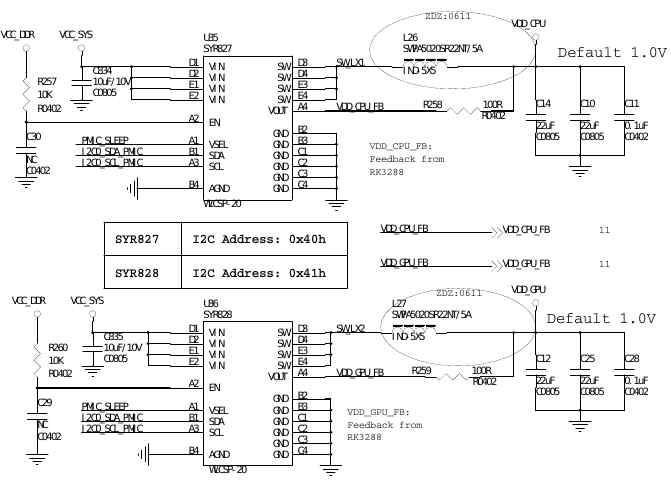
ACT8846 with SYR827 and SYR828 companion ICs
This PMIC is used typically in conjunction with the 28nm Rockchip RK3288, and full schematics may be found by searching for "T-Firefly" and also "EOMA68-RK3288". Like the AXP209 it is an integrated PMIC but it does not handle battery charging or VBUS detection and OTG triple-way power switching.
It does however, in combination with the SYR827 and SYR828, handle a lot more power than the AXP209 (2.8A for two of its DC-DC converters). The SYR827 and SYR828 are used on the RK3288 to provide the SoC core domain power and the GPU core power, respectively. The default voltage is 1.0 volts and may be reduced or increased under I2C control as needed.
AXP803 and companion MOSFET for Battery
The AXP803 handles a lot more current and has a lot more options than the AXP209: it's a bit larger, a bit more expensive, but is specifically designed for modern quad-core SoCs. It can also handle a lot more current for charging because the battery MOSFET is an external IC.
The A64 for which this PMIC was first deployed is a 40nm quad-core SoC, so the default power domains are designed specifically for that SoC.
Control Signals include:
- I2C for control, access to GPIO and selection of voltages on all outputs
- 2 GPIOs which may be switched to an additional pair of LDOs
- NMI# - Non-Maskable Interrupt. Critical to be connected to the SoC.
- RESET# - a reset signal
- PWR-ON - press or press-and-hold, used for hard power-cycling of the device
- USB-DM/DP - this is to detect the presence of an OTG device in a clean way
- USBVBUSEN - just as with the AXP209 this controls power to the OTG port.
The AXP803 has additional capability to detect whether a USB 3.0 OTG Charger has been connected (so that additional current may be negotiated). This is most likely the reason why the USB+/- lines have to be connected to the PMIC.
Outputs include:
- 6 DC-DC converters
- 3 ELDOs (extremely low-dropout outputs, for high-stability)
- 4 DLDOs (digital LDOs)
- 3 ALDOs (separate LDOs for Analog supply)
- 2 FLDOs (no idea what these are: refer to the datasheet)
- Dedicated RTC VCC supply
Overall it is an extremely sophisticated PMIC which has the advantage of being mass-produced, proven (just like the AXP209 before it), and significant linux kernel driver support that is well-understood.
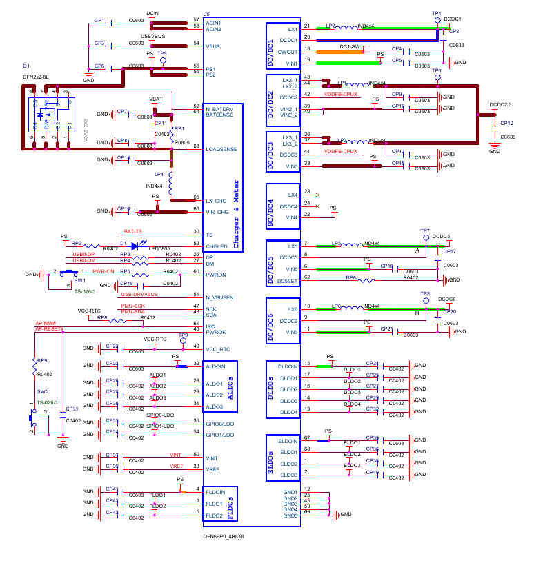
Ingenic JZ4760 PMIC Approach: Discrete ICs
The team that did the Ingenic JZ4760 LEPUS Reference Design decided to take a different approach to Power Management: multiple discrete ICs for each power domain. They selected multiple RT8008 ICs and used different resistors to set the required current (which is then not adjustable, but the jz4760 is so low power anyway that this doesn't really matter), and used RT9169 and other 3-pin LDOs for the RTC and low-power 1.2v supply.
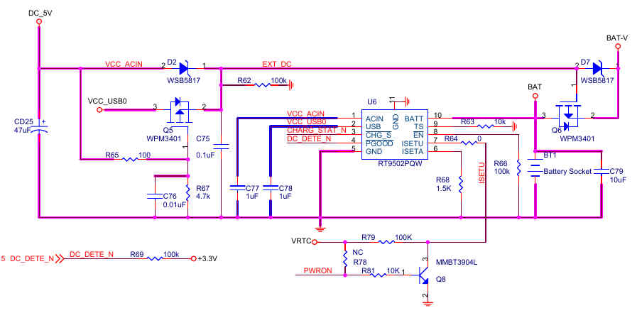
Of particular interest is how they did battery charging and the USB OTG power-switching. For the battery charging including being able to charge from either a 5V DCin or the OTG VBUS, they selected the RT9502. A MOSFET protects against power input from VBUS fighting with DCIN, and a Schottky Diode protects against current fights. A second MOSFET and Schottky Diode allows power-selection of either battery or DCin to the RT9502. All in all it's quite a sophisticated and clever circuit.
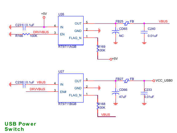
USB Power Switching - selecting between either 5V or VBUS to go in (or out) of the OTG Port without blowing anything up - is done with a matched pair of RT9711A and RT9711B ICs. A SY6280 has not been deployed, so it is not precisely clear which IC does the current-provision / over-current protection on the OTG port.
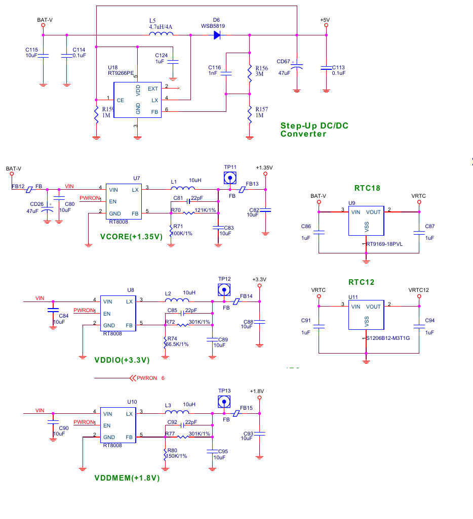
In addition to these discrete ICs for power provision, there is the usual step-up converter (an RT9266) which converts the 3.8-4.2v battery directly into a stable +5V supply. This is fairly normal, and can be seen in pretty much every design (whether using the AXP209, AXP803, ACT8600, ACT8846 and so on). It is very interesting in this case however to note that the DCin is wired (via the two MOSFETs and Schottky Diodes) directly to BAT-V (and thus supplies the +5V rail) but that, thanks to those MOSFETs and Schottkys, if either VBUS powers up or the battery powers up, they replace the power stream to BAT-V in a priority-cascade.
This example is included to show that power-provision can be done without a dedicated PMIC (but also demonstrating quite how many components it actually needs, to do so). Perhaps it might even still be a viable solution, by replacing some of the discrete (fixed) SY8008 LDOs with SYR828 and SYR829 I2C-controllable high-current voltage regulators.
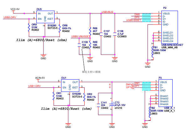
USB-OTG and USB-Host Ports
This section covers how to set up an OTG port and a plain USB2 Host port. The USB Host is quite straightforward: protect the power with a SY6280 which performs current-limiting and also stops over-voltage from the USB port bleeding back down into the 5V supply (if someone does something silly like connect a 5.5v or 6v PSU to the USB port), and that's basically it, apart from one note-worthy fact that the SY6280 may be enabled/disabled under the control of the SoC in order to save power or to carry out a hard-reset on USB devices.
The OTG port is slightly different. Note that there are 2 power lines and 3 I/O signals involved:
- VCC-5V input - for when power is supplied to the USB port (OTG Host)
- USBVBUS - for when power is supplied by the USB port (OTG Client aka usually "OTG Charging")
- USB-ID - for OTG negotiation of which end is to be Client and which Host
- VBUSDET - a resistor-divider bridge allowing the SoC to detect USBVBUS on/off
- USB-DRV - enables or disables the VCC-5V power supply (but does not affect, involve, or otherwise stop VBUS - outgoing or incoming)
It is a good idea to place the USB-DRV under the control of the PMIC, so that it may detect when a charger is plugged in, even if the main SoC is powered down. Bear in mind that this all is a cooperative arrangement where the SoC and the PMIC must collaborate to prevent power-loss and current bun-fights. VBUSDET must be arranged so that the resistor-divider bridge creates just enough of a voltage to trigger an EINT-capable GPIO on the SoC with a "HIGH" or "LOW" digital level (not an ADC in other words).
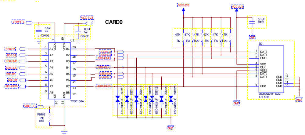
Level-shifted MicroSD
For instances where the GPIO voltage of the SoC's I/O is not 3.3v, the deployment of a level-shifter is needed. Note the inclusion of ESD protection (which needs to be very close to the SD card slot) and the 47k pull-up resistors. Strictly speaking the Card Detect line (which is an Open Drain) need not be routed through the level-shifter, whereas the SDcard signals, which are push-push high-speed, definitely do. Many "Arduino-style" amateur-deployed level shifting techniques are in fact Open-Drain style and really do not work properly as they rely on the internal capacitance of pins and tracks to drop towards Ground levels: this simply doesn't happen quickly enough, corrupting the signal integrity and is why push-push was invented in the first place.
This schematic could actually be dynamically converted to adjustable 3.3v/1.8v by replacing the level-shifter VCC-3V3 input power (U2, VCCB) with a power source that is under the control of the SoC. When the SoC detects that the inserted card has 1.8v capability, the SoC could then drop the level-shifter's B side down from 3.3v signal levels to 1.8v levels... all without having to adjust the actual SoC GPIO levels. The down-side: level-shifter ICs are around USD $1, take up a lot of board space relatively speaking, and require double the number of pins as I/O signals.
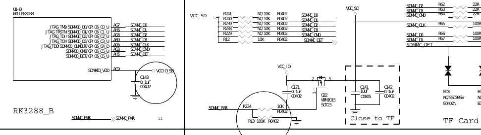
Power-domain-controlled MicroSD
This second circuit is much simpler in principle yet may still adjust the SD/MMC power levels from 3.3v to 1.8v as required. Also note that the SD Card itself may be powered down under the control of a GPIO signal (named SDMMC-PWR) from the SoC.
The level-shifting trick however in this case relies on the capability of the SoC and requires the cooperation of the PMIC. A specific LDO output from the PMIC is dedicated to this one SD card, and the entire power domain for this particular GPIO-bank (which happens only to have SD/MMC on it) is flipped from 3.3v down to 1.8v if needed.
Note that whilst this GPIO voltage domain power-drop occurs the actual SD card itself is still supplied by 3.3v. Also note that in this circuit the SD-Det is still powered from SDIO (3.3v) so the SoC GPIO will need to be 3.3v tolerant even when it is dropped to 1.8v signalling levels.
The alternative scheme would be to have an on-board level-shifter where the SD/MMC signal levels (only) are shifted between 3.3v and 1.8v levels, whilst leaving the rest of the entire GPIO bank's voltage levels alone. This seems inordinately overcomplex.
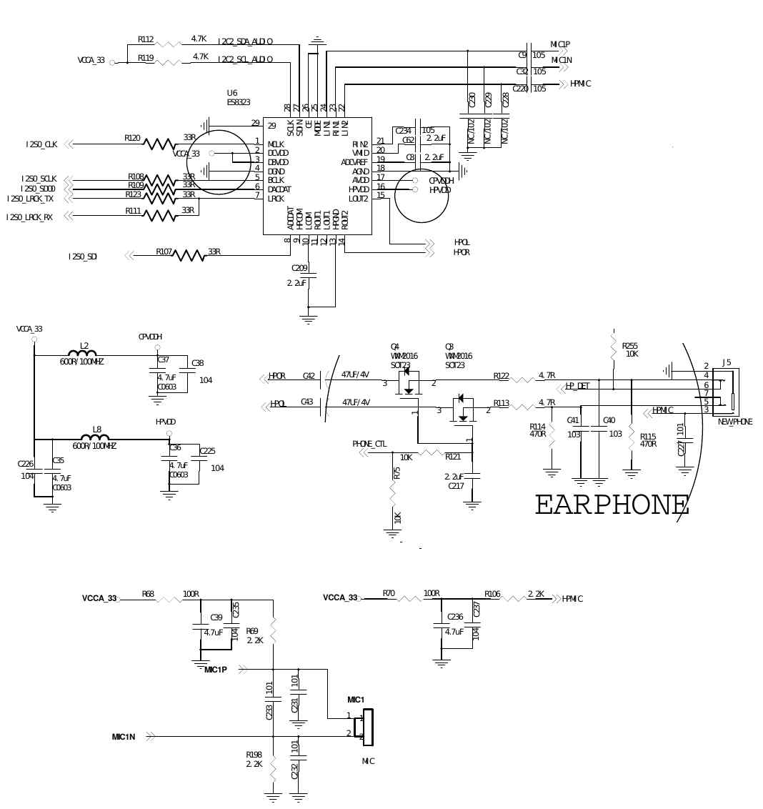
AC97-compliant (I2S) Audio
Under certain circumstances, USB Audio may be preferred over I2S (the CM108AH is a very good low-cost choice that is still mass-produced and has full schematics and no NDAs required). However USB bulk audio framing introduces latency that may prove intolerable under certain high-end circumstances (Media Centre for example). I2S was designed for low-latency and high-quality Digital Audio, send and receive.
An example AC97-compliant Audio IC is the ES8323. In this instance it is a very low-cost one (around $0.50 for single quanties from multiple vendors on taobao.com), that only has a single stereo earphone output and a single mono microphone input. For ultra-low-cost applications this is perfectly fine, considering the price and high availability. Also, using the right type of stereo headphone jack (a PJ-0345 6-pin) it becomes possible to hard-switch (and detect - using another of the precious EINT lines to the SoC) stereo headphone jack insertion and to route both outputs, via the headphone jack, back to a pair of low-cost audio amplifier ICS (TDA2822), the important thing being that this requires no additional signals or involvement or wires to/from the AC97 Audio IC. It's crude but effective: the only thing needed to watch out for is to make sure that the jack insertion (or removal) is properly detected and that the audio volume level adjusted in sufficient time (if needed). Careful inclusion of the right resistor-divider bridges etc. can mitigate even against needing to do that.
Control signals to the ES8323 are:
- 5-pin I2S: this includes, in this example, only one DO and only one DI.
- I2C: used to control the ES8323 (volume, configuration)
Audio signals are:
- Mono Microphone input
- Stereo Headphone
Many more sophisticated examples exist, which include 5-lane I2S (4 output, 1 input) for Dolby 5.1 and 7 Surround Sound, multiple audio paths including Line-out, Line-in, Car Stereo, etc. etc. - one obsolete one that was extremely good was the Akai AK4641 used in the HTC Universal clamshell / micro-laptop smartphone. All in all it just depends on the application but the actual signals / buses involved remains pretty much the same in all cases: I2S for Audio data, I2C for control of the IC (AC97 volumes and routing etc.) and optional GPIO for detection e.g. of physical insertion of headphone and other jacks. That's about it.

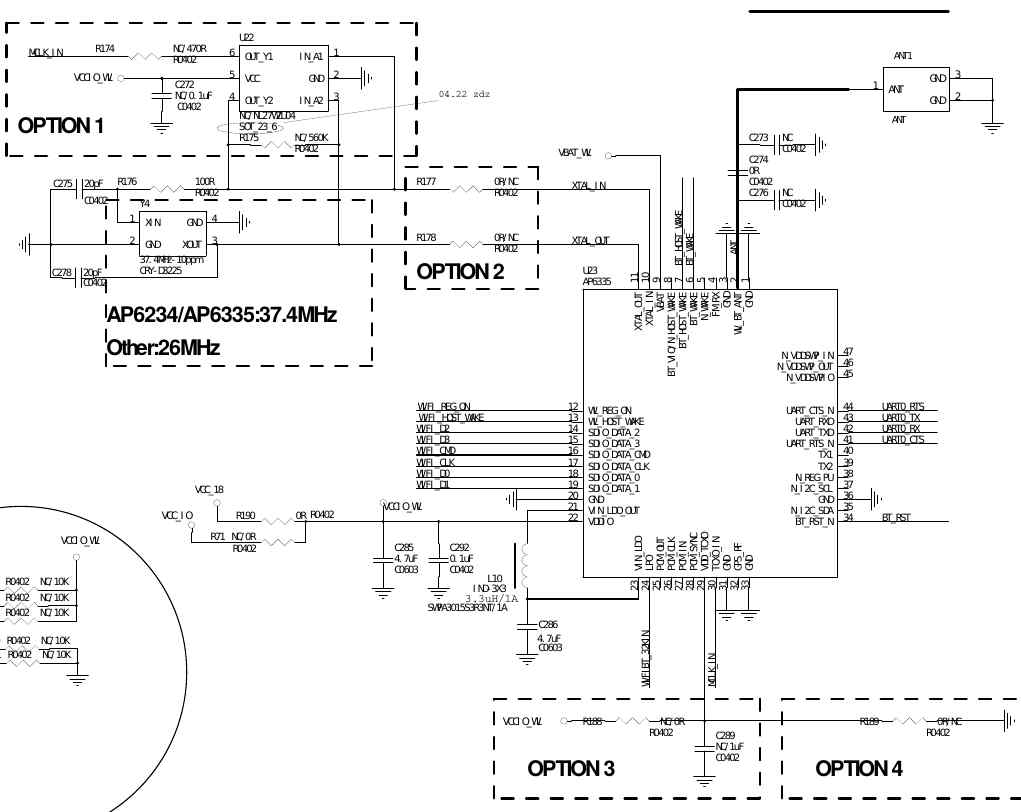
802.11 WIFI and BT
WARNING: there are NO low-power embedded WIFI ICs that are RYF-Endorseable. ALL firmware for ALL embedded (SD/MMC) WIFI SIP modules and ICs are proprietary and cannot in any way be trusted not to compromise a machine through built-in factory-installed spying, or hardware level malicious hacking (this is not a theoretical concept: it has been successfully demonstrated by Security Researchers, numerous times on numerous chipsets and numerous architectures and OSes). If you include a hard-wired SD/MMC embedded WIFI SIP module hard-soldered to a PCB it is a sure-fire GUARANTEED way to 100 percent FAIL RYF Endorsement and Certification. If RYF Endorsement and the safety and privacy of end-users is important, ensure that the WIFI module may be REMOVED (physically by the user or simply not installed at the factory) and USB-based WIFI such as the ThinkPenguin TP150N, a small 802.11abgn WIFI dongle, inserted into the device instead (either internally or externally) with the end-user having the right to remove it.
With that huge warning out of the way, we can move on to describe the signals required for an example 802.11a/b/g/n/ac WIFI and BT 4.0 SIP Module. These are:
- 4-lane SD/MMC for the WIFI data. This is standard for low-power SIP WIFI
- 4-wire UART for Bluetooth, including TX/RX as well as CTS/RTS.
- Quite a lot of IRQ and communication lines: up to five EINTs and GPIO in the case of this particular SoC.
The GPIO lines particularly EINTs are critical for WIFI and Bluetooth, particularly as applications may be adversely affected by clashes of these two protocols sharing the same 2.4ghz frequency bands. So the OS needs to know when a clash is detected, immediately: that requires an EINT-capable GPIO, on its own. Also, BT or WIFI (separately) may be used to wake up a host that has been placed into low-power sleep mode: again, that requires two separate and distinct EINT-capable GPIO lines.
This particular WIFI SIP module also takes a 32.768kHz RTC input signal (which may be generated by the SoC or by a companion MCU), and it is also recommended to dedicate an additional GPIO to a MOSFET or other means to hard-kill the entire WIFI module.
So on the face of it, it seems very straightforward, just route SD/MMC and UART, but it's actually quite involved. It would seem, then, that deploying a USB WIFI module would be a much simpler idea, especially given that USB2 is only 2 wires (plus power) and things like "wakeup" and "signalling" etc. are typically handled (with the common exception of protocol-clashing) via the provision of features built-in to the USB Bus Protocol. The down-side: most USB2 WIFI dongles, modules and chipsets are simply not designed for low-power scenarios, not at the hardware level and certainly not at the firmware level.
Only one (modern) USB chipset - which only supports 802.11abgn and not ac - has full firmware source code available under Libre Licensing, thanks to ThinkPenguin's tireless efforts: the Atheros AR9271 USB Chipset. ThinkPenguin spent two years walking Atheros through the process of releasing the full firmware source code, and it is the only chipset where peer-to-peer mesh networking has been added by the Free Software Community, and it is the only chipset that could be considered for adjusting the firmware to reduce power consumption. Time however is running out for this chip because Qualcomm subequently bought Atheros, and Qualcomm replaced the entire management with people who completely fail to comprehend what made the AR9271 so very successful.
Bottom line: WIFI and Bluetooth are an ethical minefield as far as user privacy, rights, and hardware-level remote hacking are concerend, and it starts right at the early design phase: component selection. A good way to ensure that users have control over their own devices is to add hardware (physical) kill-switches to the power lines, and/or to allow them to actually physically and completely remove the WIFI / BT module without invalidating the warranty.
Datasheet: http://www.t-firefly.com/download/firefly-rk3288/hardware/AP6335%20datasheet_V1.3_02102014.pdf
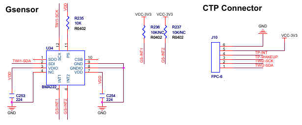
I2C Sensors
I2C sensors appear on the face of it to be quite straightforward: wire them up to the 2-line I2C bus and it's done, right? It's not that simple: I2C is a master bus only, meaning that if the peripheral has important data, it has to have some way of letting the SoC know that something's happened. This requires an EINT-capable IRQ line on the SoC in order to wake up the SoC from tasks or low-power mode(s). In addition, it's often the case that the sensor may need an occasional (or a definitive, on start-up) RESET. In particular it's a good idea to reset sensors after power-on due to potential problems caused by in-rush current instability: often this is covered in the datasheet as being required.
So typically for each sensor, two extra GPIO lines are required: one EINT and one not. If the amount of GPIO begins to run out (EINTs are usually a finite resource) then it is technically possible to share SoC EINT lines using logic gates (one for a group of sensors), board-space permitting. The other technique is to use a companion MCU for EINT aggregation, and even, if pins are particularly sparse, to use the fact that the USB Bus has built-in wake-up capability to the SoC. A signal (or the actual data if the sensor is directly connected to the MCU instead) can be sent over USB. Typically in this instance it's a good idea to use the MCU to convert to a more standard format such as presenting one or more USB-HID endpoints (for CTP, Trackpad and mouse-like sensors), otherwise a special linux kernel driver needs to be written.
Other than that, sensors are pretty straightforward. Most already have a linux kernel driver already available. If they don't, they're best avoided: pick another one that does, as it's a sure-fire sign that the sensor has not seen mass-volume production deployment, or if it has, there's been zero opportunity to do a security review of the source code and/or it'll be GPL-violating.
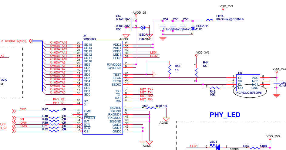
Ethernet PHY IC
The normal standard for Ethernet PHYs is MII (10/100) and its variants, GMII (10/100/1000 Ethernet), RGMII and so on. There is however a different approach: MCU-based interfaces. In this particular instance, the Shakti team have already created a FlexBus implementation, which can be used to emulate the required SRAM / 8080-style micro-controller interface needed. A number of MCU-based Ethernet PHY ICs exist, including the AX88180 (which is a Gigabit MCU-to-RGMII converter), the AX88796A (a 10/100 PHY which supports 8080 as well as MC68k-style interfaces), and the low-cost and well-established 10/100 DM9000 PHY. It requires the following signals:
- 16-bit Data/Address Bus
- CMD select (Changes bus from Data to Address lines)
- PWRST# (Power-on Reset)
- IRQ (Interrupt indicator from DM9000 to SoC)
- IOR# (Read Ready)
- IOW# (Write Ready)
- CS# (Chip Select)
This comes to a total of 22 GPIO lines, which is a significant amount. However it is also possible to run the DM9000 bus at a reduced 8-bit width (with a slightly different pin arrangement for the top 8 bit pins: see datasheet for details), for a total 14 pincount. In addition, as a general-purpose shared memory bus it's possible to connect other peripherals simultaneously, mitigating the high pincount issue, requiring only one Chip Select line per peripheral. For example, if two Ethernet PHY ICs are required they may be placed on the exact same Bus: only one extra CS# line is required, and the pincount is now 15 pins for two Ethernet PHY ICs: a much better average pincount ratio than would be achieved from using two RGMII PHYs.
Other important details: the AX88180, AX88796A and the DM9000 all have had linux kernel and u-boot driver source code available for many years.
Datasheet: https://www.heyrick.co.uk/blog/files/datasheets/dm9000aep.pdf
USB-based Camera IC or Bit-banging CSI
Low-cost Cameras typically require either a MIPI interface (CSI-2) or a Parallel Bus-style interface (CSI-1). Theoretically it is possible to bit-bang the CSI-1 interface, using a PWM for generating the clock, reading the HSYNC and VSYNC signals and the 8 to 12-bit data, and even using DMA to optimise the process. For an example implementation of this techique see https://www.nxp.com/docs/en/application-note/AN4627.pdf
However the DMA / bit-banging technique takes up at least 12 pins, 14 if the I2C interface is included, and many sensors require a minimum clockrate (data-rate) of 12 mhz before they will respond. A way to greatly reduce pincount is to use a USB-based IC, such as the low-cost, mass produced VC0345 from VIMicro.
The VC0345 can do up to VGA @ 30fps, and can take still pictures up to 3M-pixels so is not exactly the fastest bunny on the block, but it has the distinct advantage of not requiring an NDA to gain access to either the datasheet or the app notes, and it is so commonly available that approaching the manufacturer is not actually necessary: it can be obtained directly from Shenzhen Markets. Also as it is a UVC-video compliant device, linux kernel driver support is automatic.
An alternative approach to using an off-the-shelf CSI-to-USB Camera IC is to use a companion MCU: after all, the VC0345 is just a general-purpose 8051 MCU. A student achieved this with an ultra-low-cost Camera Sensor (QVGA) and an STM32F103 back in 2010: https://github.com/adamgreig/negativeacknowledge/blob/master/content/from-wordpress/robot2-an-arm-based-colour-tracking-robot.md
However for coping with larger sensors, care has to be taken: not least, it is not possible to fit an entire sensor frame into the SRAM of a small MCU, so there has to be some care taken to avoid loss of data. Also, the MCU must have 480mbit/sec USB2 capability, as beyond around 640x480 even at 15fps a USB 1.1 11mbit/sec bus becomes completely saturated. Also to watch out for is whether the MCU's USB hardware supports enough simultaneous endpoints, particularly if USB-HID for keyboard (matrix to USB-HID keyboard) and/or USB-HID trackpad (mouse) or other devices are to be managed by the same MCU. Those caveats in mind: it is actually achievable.
- Datasheet: http://hands.com/~lkcl/eoma/kde_tablet/VC0345TLNA-1102-V10-EN.pdf
- VC0345 App Note: http://hands.com/~lkcl/eoma/kde_tablet/VC0345_app_notes.pdf
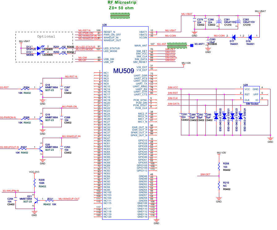
USB-Based 3G / UMTS/HSDPA Modem
GSM / GPRS / EDGE Modems are typically slow enough to be able to use a UART at 115200 baud data rates. 3G on the other hand is fast enough to warrant the use of a USB connection. Depending on the firmware, some 3G USB-based Modems offer multiple endpoints, some of which can transfer audio data. Others offer two-way duplex digital audio over a standard four-wire "PCM" arrangement. The MU509 also (as previously mentioned in relation to the HTC Universal) has GPIO pins which may be accessed over an AT command-set. Using these becomes extra-complex as far as software is concerned, so should only really be used as a last resort.
Connectivity for this particular 3G Modem is as follows, which will give the minimum functionality:
- USB2 (+/-)
- 3G Power Enable (to an LDO to cut/enable power to the entire Modem)
- RESET#
- PWRON
- WAKEUPIN# (to wake up the 3G Modem)
- WAKEUPOUT# (for the 3G Modem to wake up the SoC: requires EINT-capable pin)
- SIM Card (connected to the MU509, not the SoC)
This is a minimum of 5 GPIO plus 2 USB lines. Optional extras include:
- Full UART (TX/RX, CTS/RTS, DTR/DCD/DSR, RING)
- PCM 4-wire audio (standard WAV format, supported by many Audio HW CODECs)
- Twin Mics
- Speaker Out
- Headset Out
- 12 pins GPIO
Note also in the example schematic that MMBT3904 transistors have been deployed for simple level-shifting and also convenient inversion of the control signals. Care needs to be taken in reading the datasheet to ensure that the voltage levels of the GPIO match the GPIO Power Domain of the SoC GPIO Bank to which the control signals of the MU509 are connected (and level-shifting deployed if needed).
Also, special attention must be paid to the power supply: GSM and 3G Modems, particularly the "M2M" ones, require an enormous amount of current: 2 to 2.5 AMPS is not unusual. M2M modules are also typically designed to operate off of a direct Lithium battery voltage and are not to be run off of a 3.3v or 5.0v supply. Hence in the example schematic below an LP6362 high-current LDO is used. This however requires an additional GPIO, which is utilised to control the power supply of the 3G Modem.
Deploying hard-power-kill switches (physical and/or under SoC GPIO-control) is generally a good idea with USB-based 3G and GSM Modems. During long-term operation, these modems, which are basically yet another ARM Processor and their own DDR and NAND storage with a full Software Stack (often linux kernel based) inside an enclosed metal box, are pretty much guaranteed to crash so hard that they become completely unrecoverable and unresponsive, and have even been known to cause the USB Host Endpoints that they are connected to to hard-crash as well. The only way to deal with that is to hard power-cycle the Modem module in order to do a full reset of its USB PHY.
The other reason for considering deployment of a hard (physical) kill-switch is for respecting user privacy and safety. Also, it is worth ensuring that the 3G Modem does not require its firmware to be uploaded each and every time it is powered up: it's much better to select a Modem that has its own independent on-board NAND Flash (fortunately, unlike with the WIFI module industry which is the total opposite, it is standard practice to include on-board NAND on GSM/3G Modems). The hassle of getting a Modem Hardware Manufacturer to provide the exact and correct firmware per country per Cell-Operator (the FCC is particularly strict about this in the USA, and even requires FCC Re-Certification per Operating System at a cost of USD $50,000 per modem, per cell-operator, per firmware release, per OS release), all of which of course will require an NDA (for binaries??), and require MOQs of 100k units or above just to get them to answer enquiries: it's just not worth the hassle and the cost "savings" of not having NAND Flash on the actual Modem module.
Plus, uploading of software (firmware) from main OS Storage to a peripheral is something that instantly terminates any possibility of obtaining RYF Hardware-Endorsement Certification. To make that clear: as long as all peripherals (such as a 3G Modem) that run proprietary software are fully-functional from the moment they leave the factory, i.e. they do not require software to be uploaded to them via the main OS in order to do their full job, RYF Certification can be sought. Ath5k and Ath9k WIFI modules are another example of peripherals that have on-board NAND and are fully-functional from the factory, so do not stop RYF Certification.
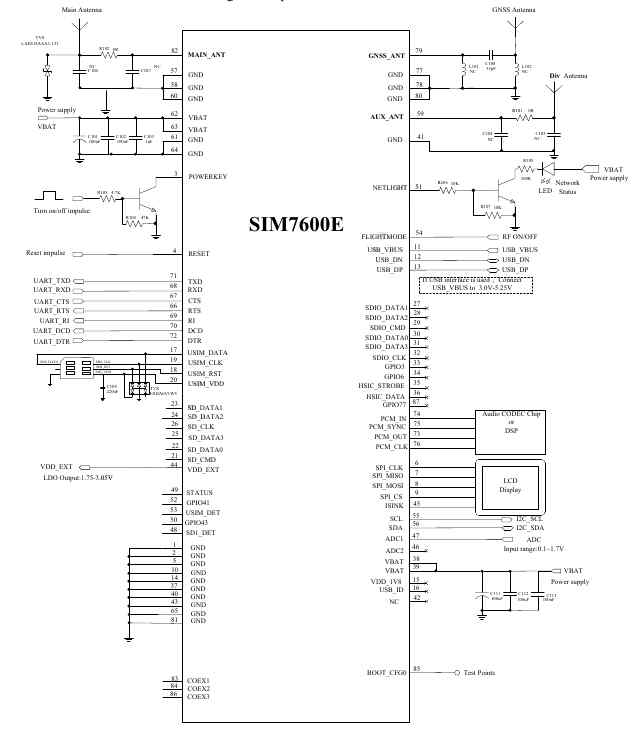
SimCOM SIM7600 / SIM7100 USB-based GSM/EDGE/3G/4G/LTE Penta-band Modem
An up-to-date low-cost Modem example is one from SimCOM. SimCOM are best known for their low-cost SIM800 and SIM900 "workhorse" GSM modems, which are extremely popular in the Shenzhen Markets. SimCom also have some LTE multi-band modems, the 7100 and 7600 Series. Full technical documents can be obtained by registering and then logging in to their website (or instead by simply searching online without registration). The SIM7600E is here: http://simcomm2m.com/En/module/detail.aspx?id=178. Checking pricing and availability, it actually seems that the SIM7100C is more popular. has lots of developer kits available, some MiniPCIe designs, bare modules, and, importantly, plenty of suppliers which is a good sign.
The pinouts are pretty much exactly the same as the Huawei MU509, with the addition of two SD Card interfaces, two ADCs, and an SPI interface for running a display. This module, it seems, is actually designed for use as a stand-alone, fully-functioning actual phone, not even requiring a companion SoC or MCU at all. The SIM7100 also supports sending and reading of Audio data over USB. The Application Notes are significant which makes it an extremely good choice. There is even advice on how to design an interoperable PCB that supports the low-cost SIM800C, the SIM5360 and the SIM7100, all of which are in the same footprint and are nearly 100% pin-compatible. Documents can be obtained without NDA from here: http://simcomm2m.com/En/module/detail.aspx?id=85